Sound on
Work in Progress
These docs are still a work-in-progress and may not be fully baked just yet! Please contact me if any of it seems very wrong or needs extra clarification.
note
Speaker terminals do have +/- sides but, for the way this one's being used, it won't matter how they're connected. Feel free to honor the "red is positive, black is negative" convention like the battery, or not! You'd be hard pressed to hear any difference.
Steps
- Solder the last vertical SPDT to SW1 and 10k potentiometer to RV2.

- Solder 220uF capacitor to C4.
- Note the cap's polarity. Match the white band on its cylinder to the white half of the PCB footprint.
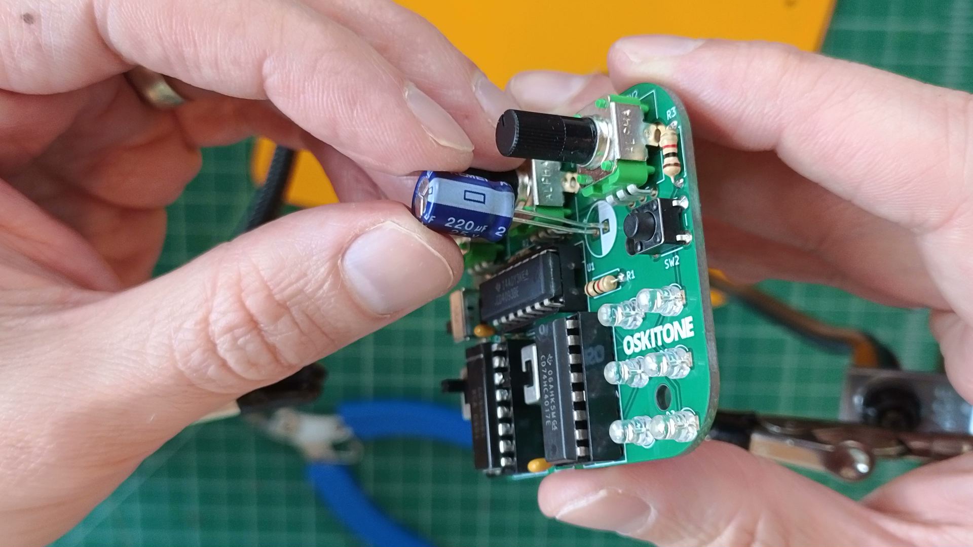
- Note the cap's polarity. Match the white band on its cylinder to the white half of the PCB footprint.
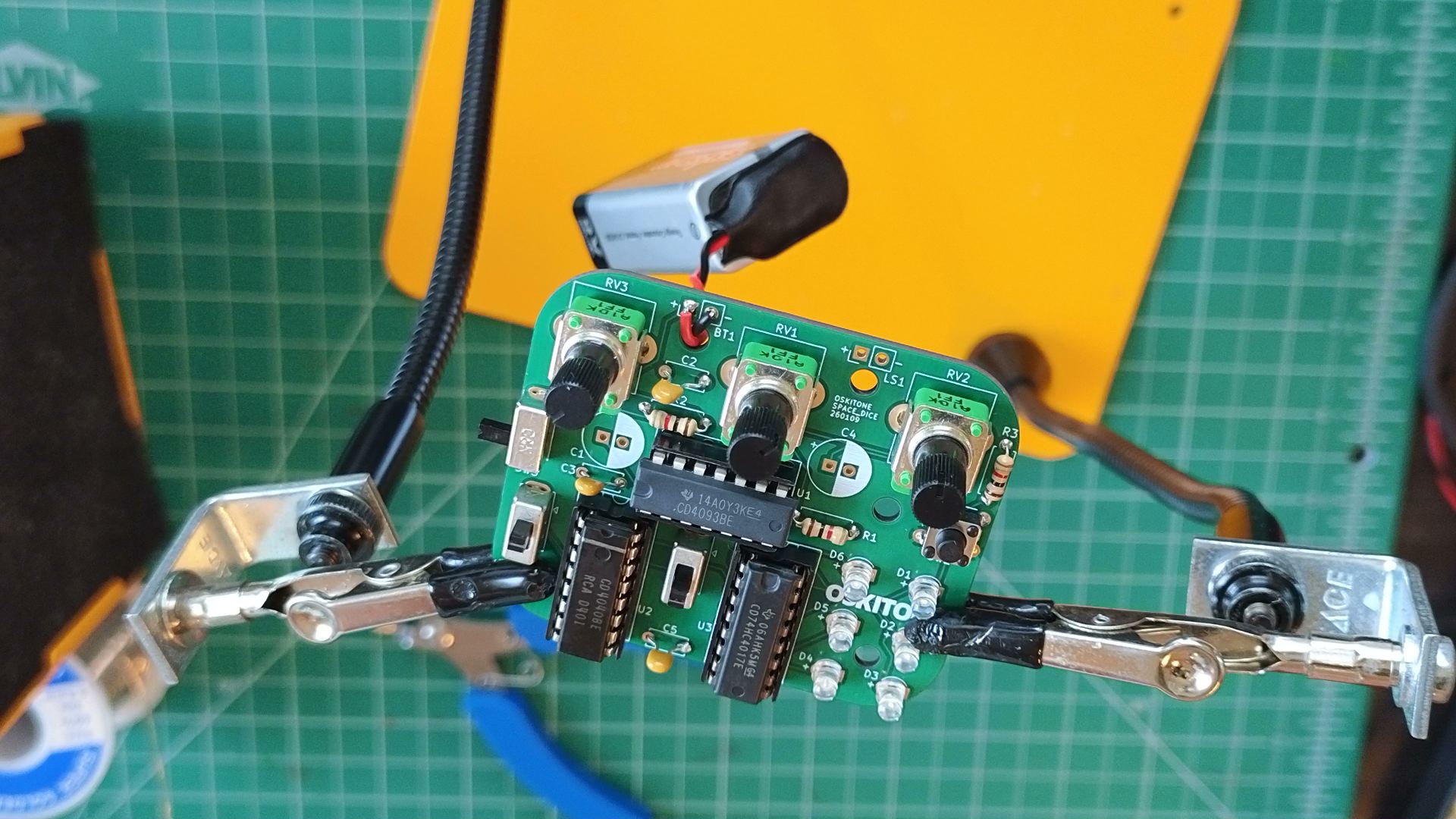
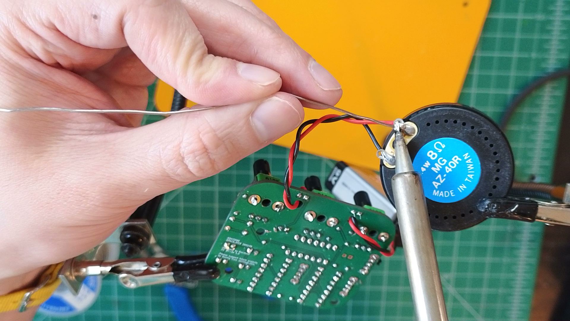
- Connect speaker
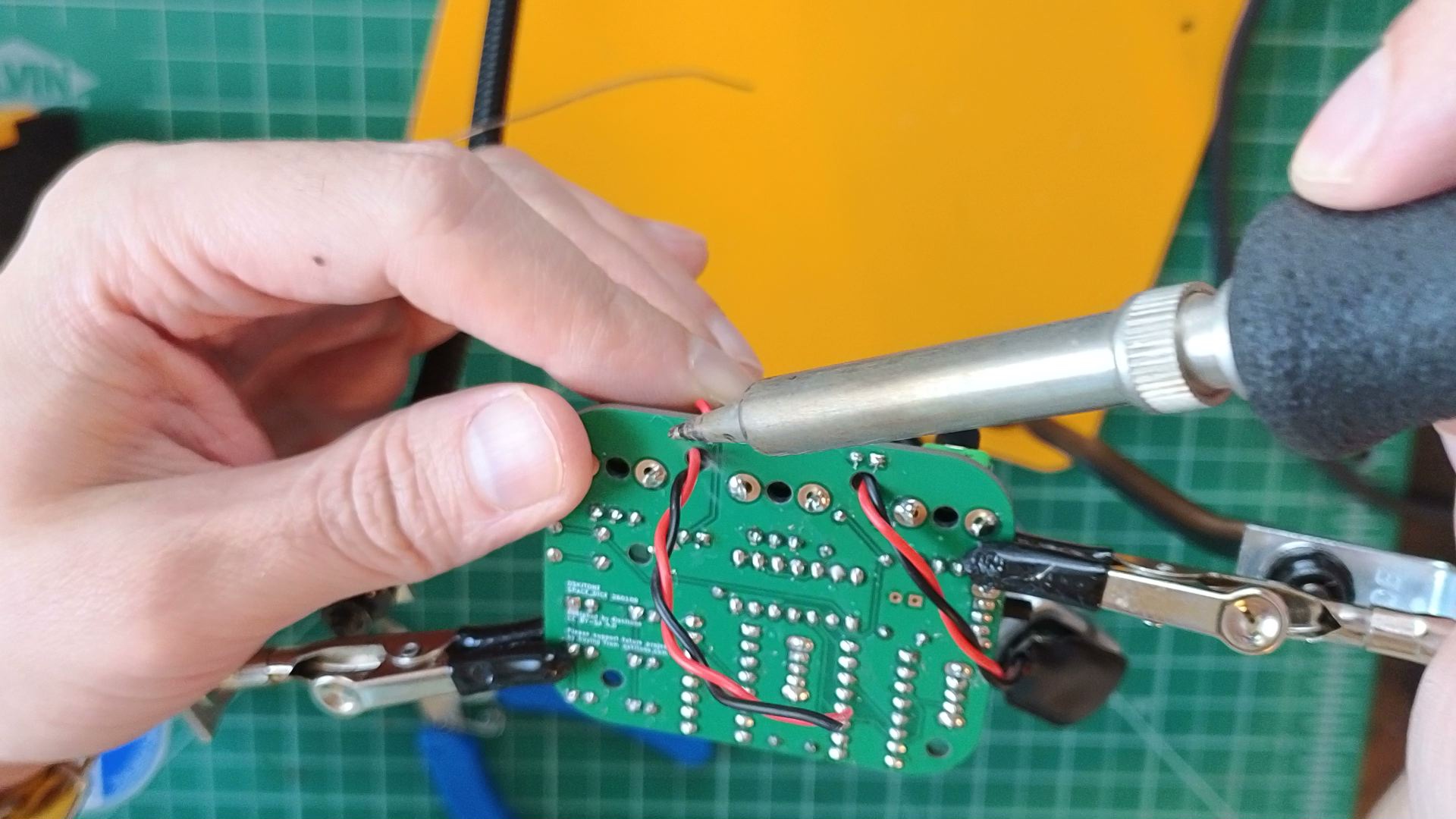
- Just like you did for BT1, feed the other half of the 9v snap's wires through the relief hole by LS1 and solder to LS1.

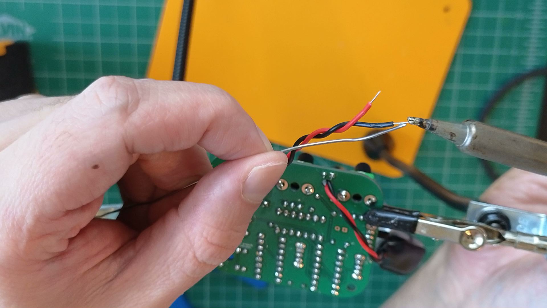
- Strip 1/4" of insulation from its other ends and "tin" them by melting some solder onto them.

- Solder the stripped, tinned ends to the speaker's terminals.

- Just like you did for BT1, feed the other half of the 9v snap's wires through the relief hole by LS1 and solder to LS1.

Test
Pressing SW2 should now also make a beeping sound. RV3 and SW1 should control pitch. RV2 should kind of control its volume (see notes below).
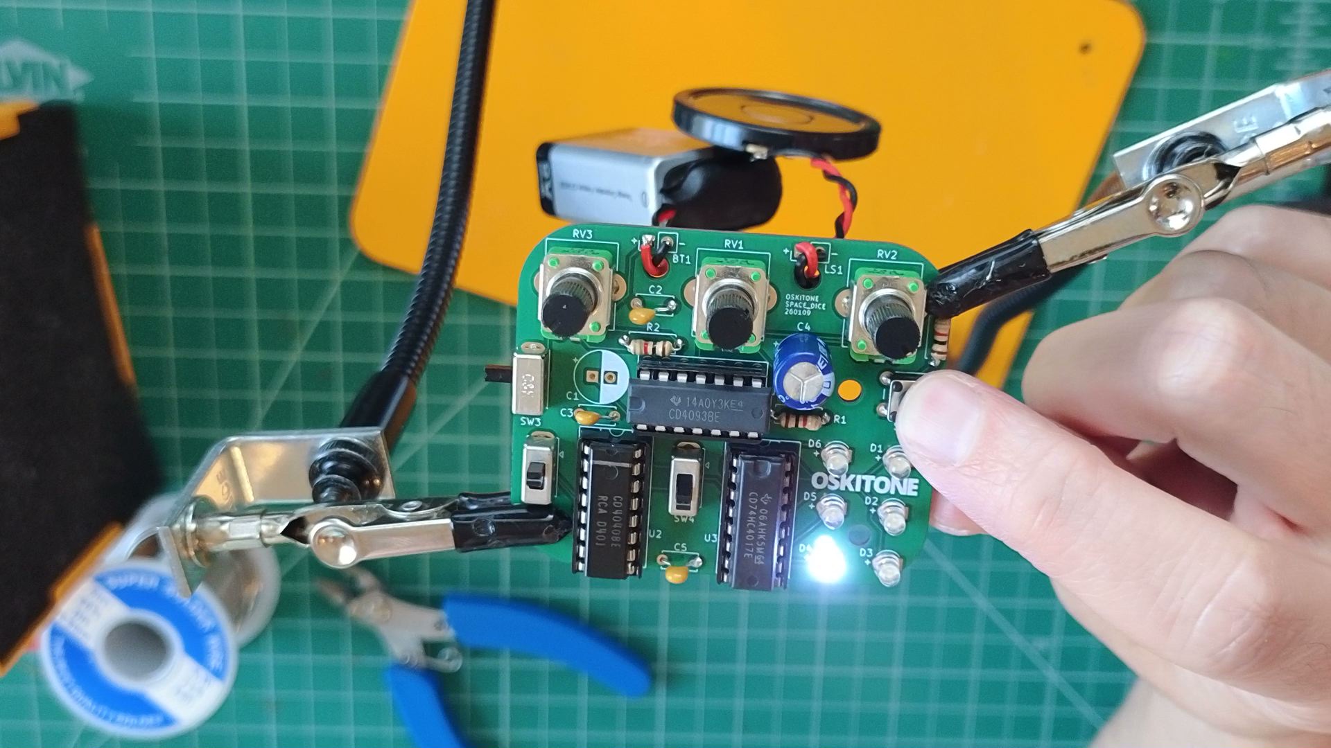
Not working as expected? Check the PCB troubleshooting section. Otherwise, continue.
How it works

- Each 4040 output pin creates a square waves at half the frequency of its predecessor. In musical terms, when a note is half the frequency of another, it's an octave down. Twice the frequency, it's an octave up. The 4040 is an octave generator!
- But how can we listen to it? If we were to connect any single output pin up to a speaker, there wouldn't be enough current to audibly drive the speaker. We need an amplifier or some way to boost the signal...
- A NAND with its inputs tied together becomes a NOT. If you connect multiple NOTs in parallel, their output current multiplies. Thus, the three remaining 4093 NAND gates make a crude inverting square wave booster. This is a hack! PCB software warns against connecting logic gate outputs; in practice, it is fine.
- Three of these octaves (two switchable through SW1) connect to the input to our booster, and its output goes through the RV2 potentiometer wired as voltage divider for volume control and then to a speaker.
- The enclosure labels RV2 as "VOL" for "volume" and SW1 as "OCT" for "octave."
- C4 is a coupling capacitor. Its job is to connect the amplified audio's alternating current (AC) to the speaker but block direct current (DC; for example, a sustained 9v). Without it, the speaker would draw more current than the 4093 could provide, eventually damaging it.
- The lines out of Q0 and Q2 are drawn crossed, but they don't connect electronically. Schematics will usually explicitly denote line/wire connections with dots, like the ones flanking the NAND gates.
- You've probably noticed that RV2 does indeed control volume, but it seems to have a wide deadband in the middle where there's no discernible change. The reason for that is that the booster hack works well enough to audibly drive a speaker but is not a proper amplifier. So we're kind of stuck with an odd compromise where the volume control works more like a switch than a pot. S'okay!
Consider:
- If the 4040 outputs square waves, what kind of waveform do you get when they're connected? (Hint: any low GND output will sink any high VCC output it contacts...) If you've got an oscilloscope, you could measure and watch the resultant waveforms.
- Inside the speaker is an electromagnet that moves the speaker's cone when electricity is applied. The cone's movement creates a wave in the air that our ears interpret as sound. Knowing this, why does reversing the polarity of its connections not seem to matter?