Power up
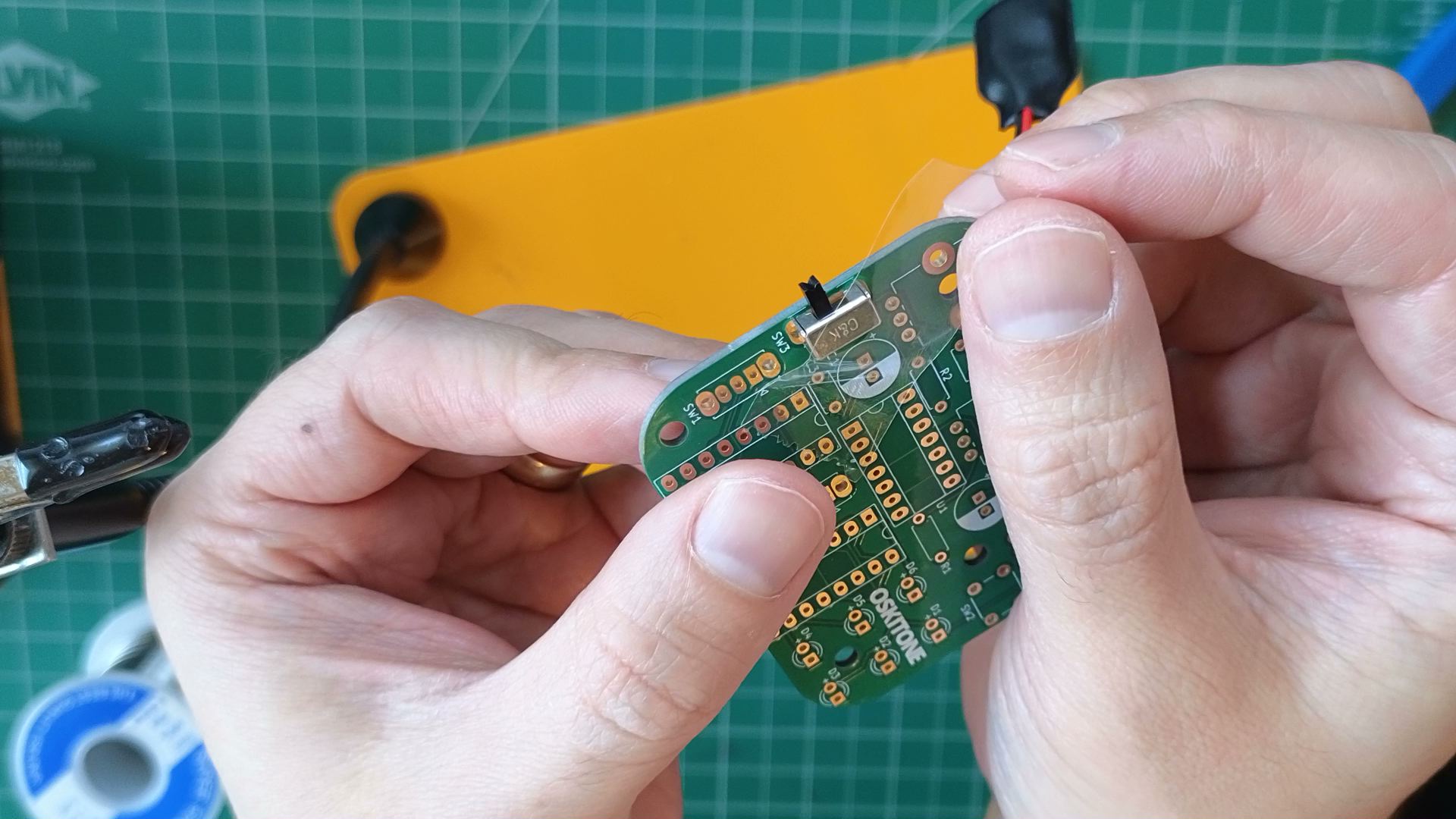
SPST switches have very short legs and won't stay in the PCB as you flip it over, making them tricky to solder. You can use a bit of tape to hold them in place as you solder. See the general tips section for other advice.
There are three SPST switches in this kit: one with its slider at a right angle to its pins and two with their slider vertically above the pins. For this step, we want the right-angle one.
Steps
- Prep wire
- The 9v battery snap connects to two separate wires. Twist them together so they're easier to manage.
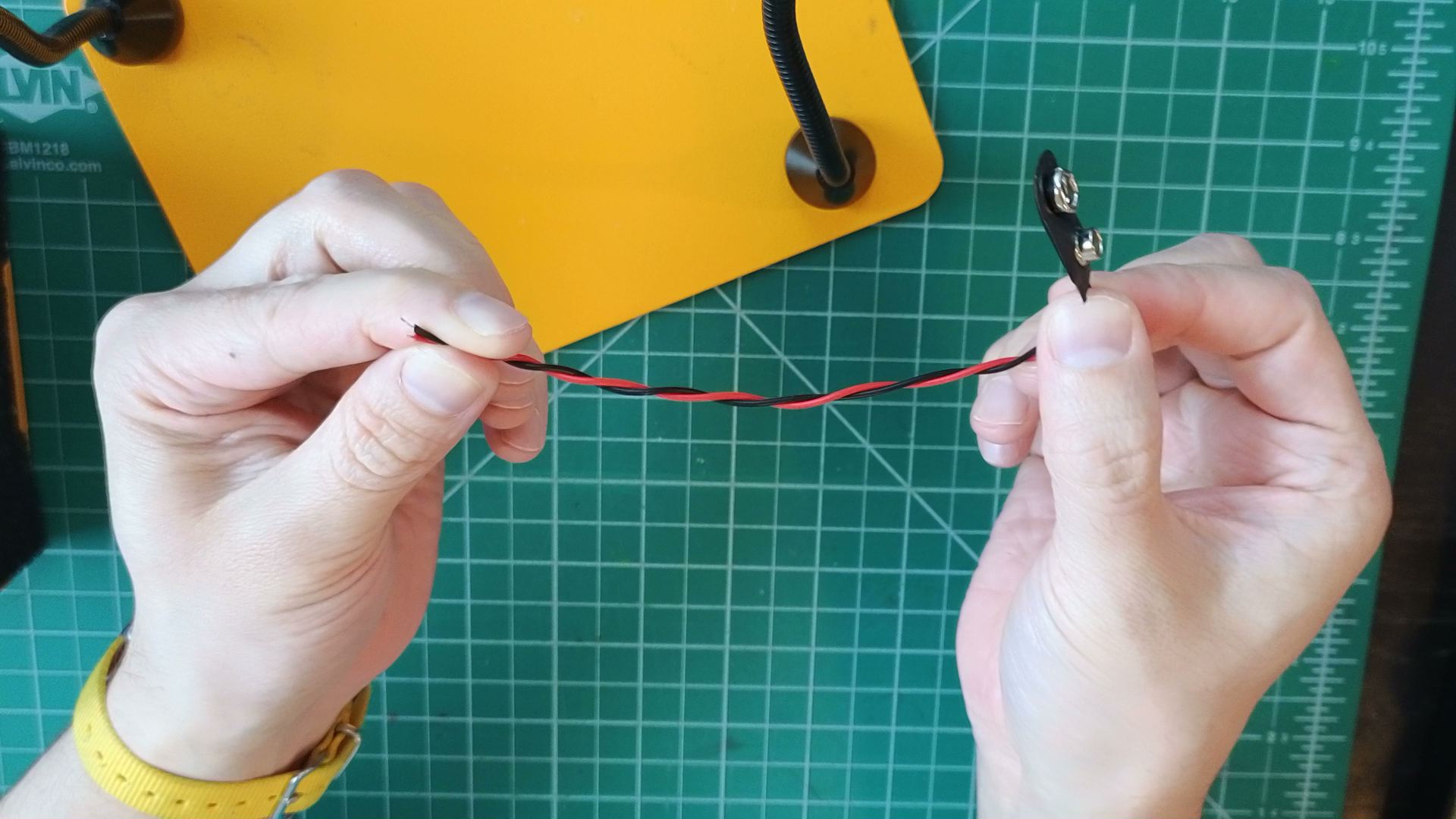
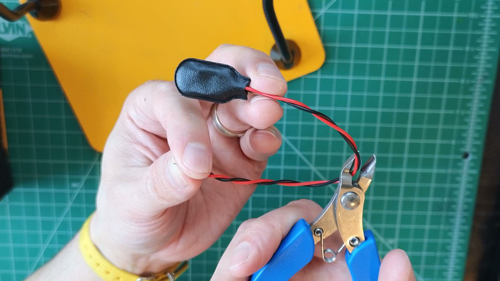
- They're also longer then needed. Cut them in half (or, minimally, 2" on the battery snap side and 1" on the other side) and save the unused section for later.
- The 9v battery snap connects to two separate wires. Twist them together so they're easier to manage.
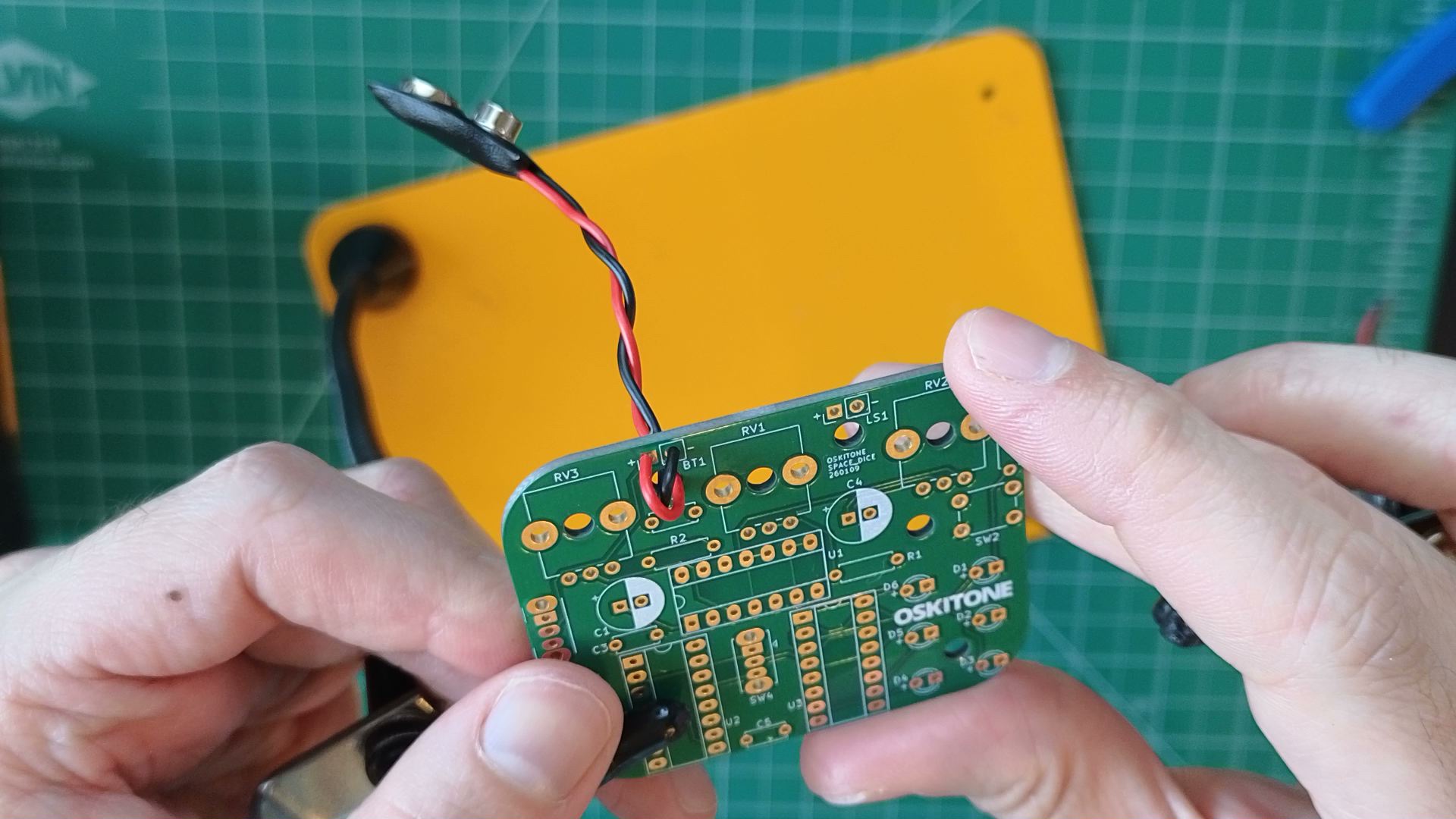
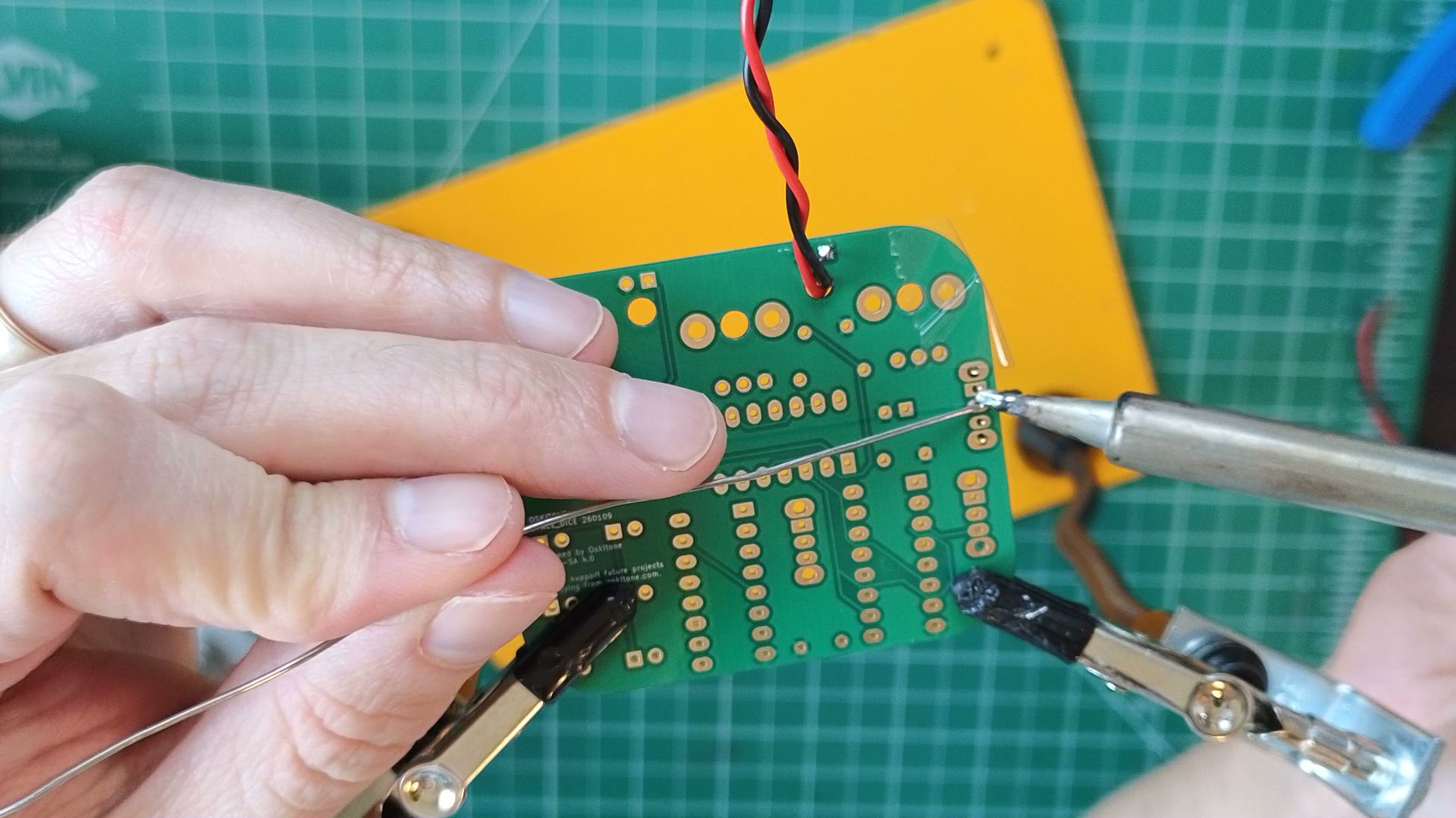
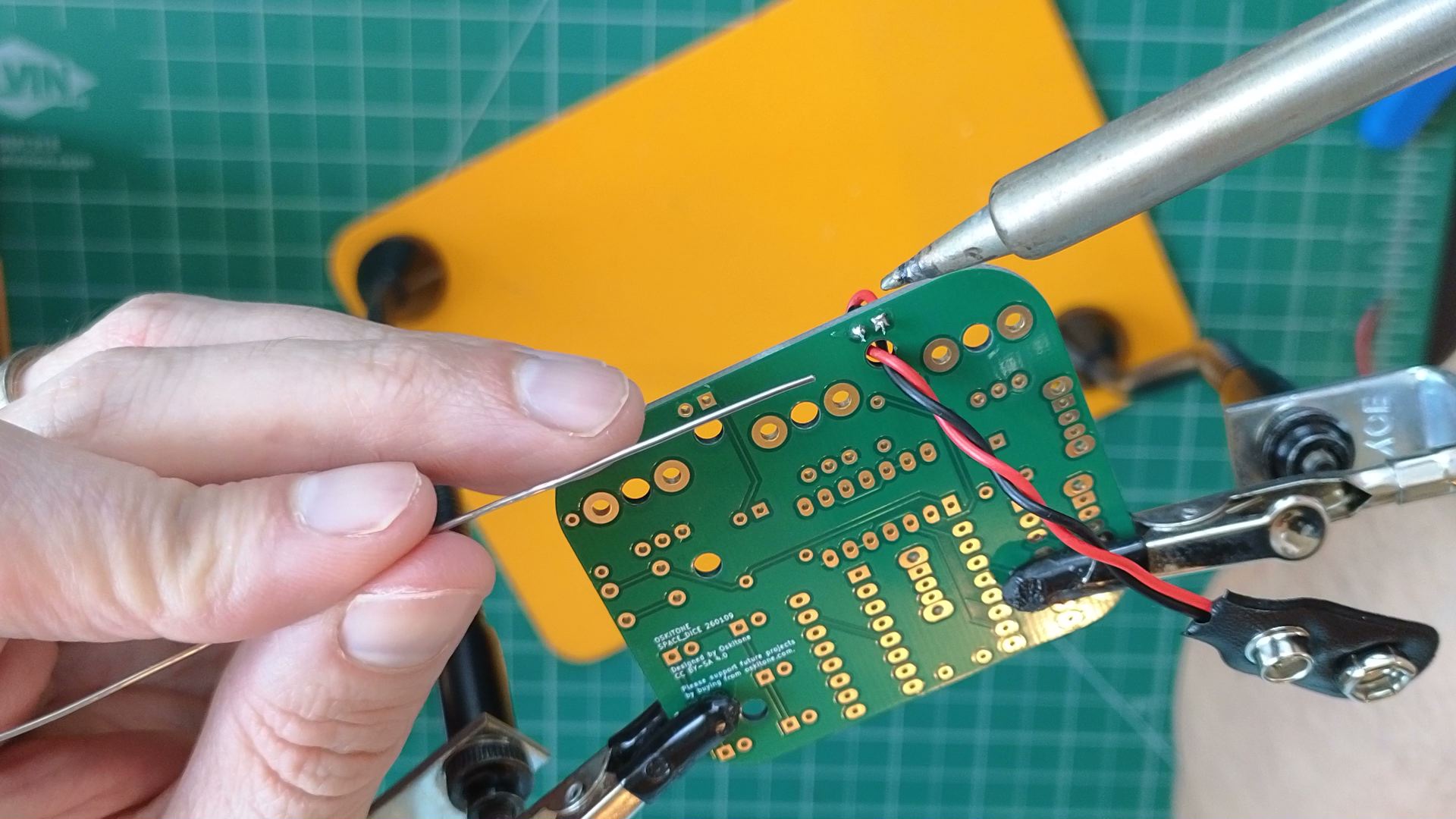
- Feed the battery snap's wires up through the relief hole by BT1, then, on the PCB bottom, solder its wires into place: red for + and black for -.

- Solder the right-angled SPDT switch to SW3. Its slider/actuator will stick off the left edge of the PCB.
- Connect a 9v battery.


Notice how you inserted components into the PCB's top and soldered on the bottom. This is standard for all the components on this board.
Test
It's okay to skip the multimeter test if you don't have one. Just keep in mind that if the next step's test doesn't pass, it may be a battery/power problem.
Use a multimeter to measure the voltage across any/all of these empty chip pins as you toggle SW3.
- U2: 16 and 8

- U3: 16 and 8

- U1: 14 and 7

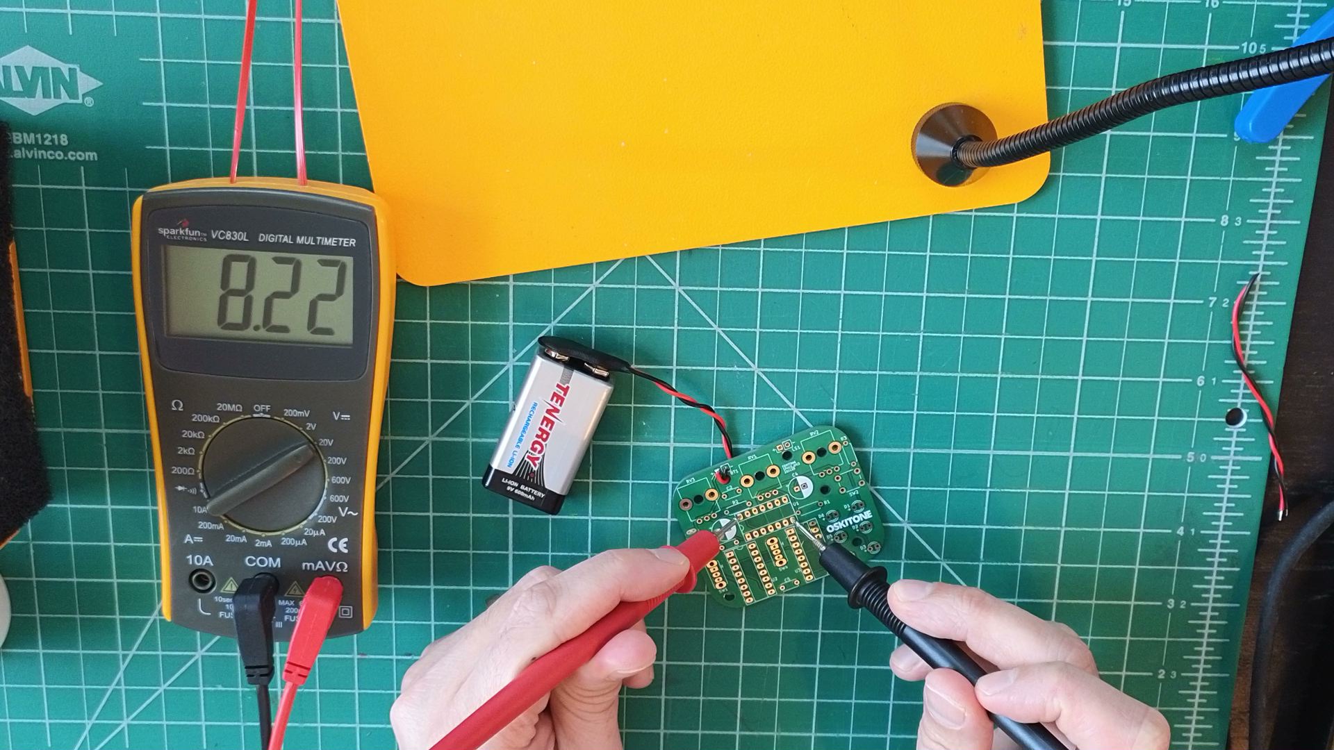
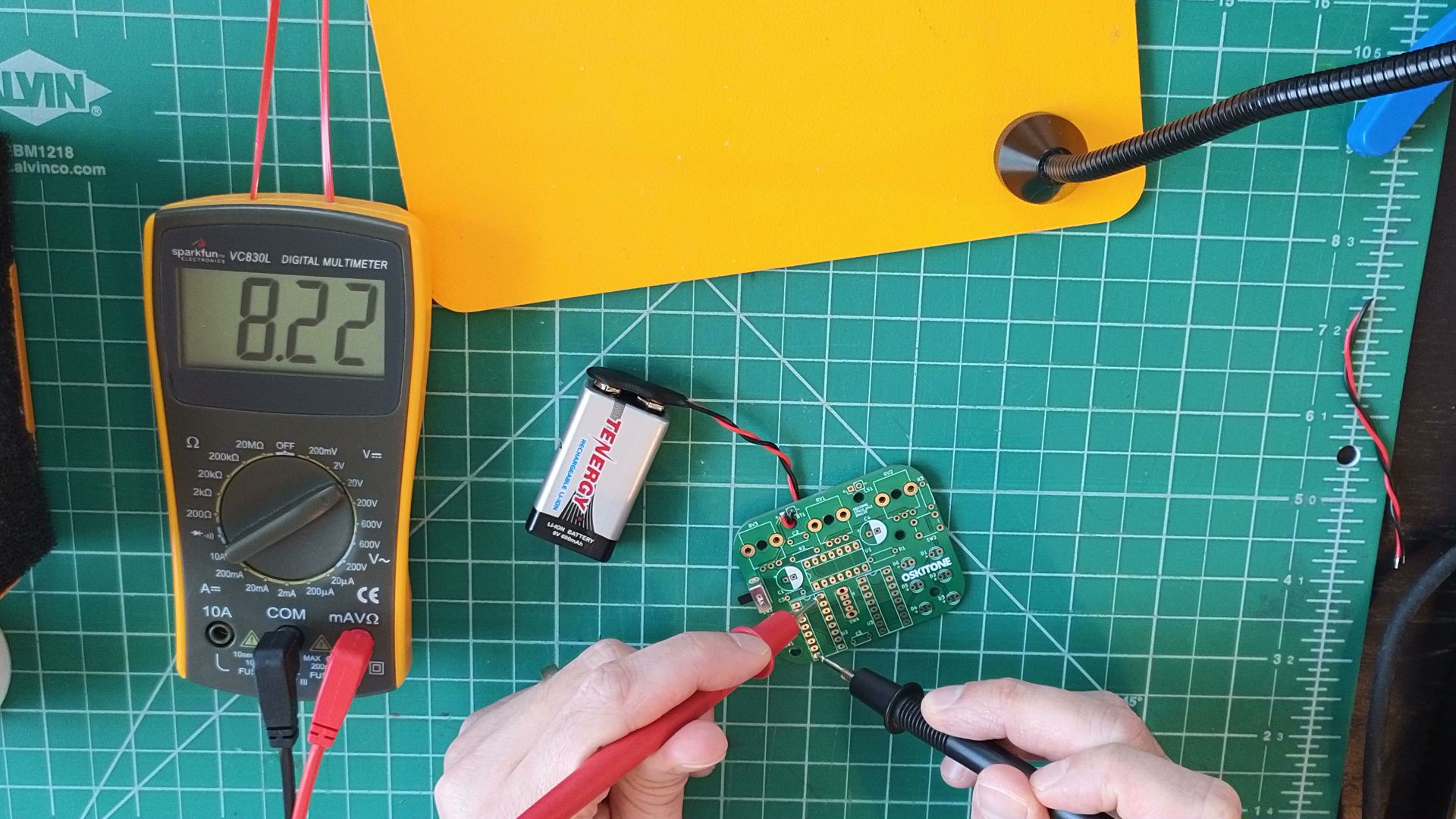
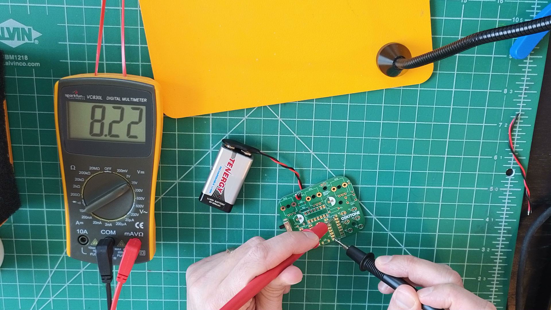
The multimeter should measure around 9v (more or less, depending on the type of battery) when SW3 is up and 0v when it's down.
Not working as expected? Check the PCB troubleshooting section. Otherwise, continue.
How it works
As you build, the presented schematic will grow with each new addition you've soldered. See if you can follow along!
Schematic symbols rarely match their physical components. You can think of them as shorthand "source of truth" for a circuit, like what sheet music is to a musical performance. Schematics tell us conceptually how to make the circuit, not what it will look like or even which specific parts to use.
The more schematics you read, the more they'll make sense.
Anyway, here's what you just made:

- BT1 is the 9v battery. Its negative terminal connects to GND (ground).
- SW2 is a Single Pole Double Throw (SPDT) switch. Its pole is the diagonal line in the middle that moves between pins 1 and 2 (the throws) as the switch slides. Its pin 2 is fixed and connects to the battery's positive terminal.
- In switch parlance, "open" means unconnected and "closed" means connected.
- You'll see VCC and GND labels throughout the schematic, and they'll all refer to the same common connections: GND will always connect to the 9v's negative terminal, but VCC and will only connect to the 9v's positive terminal when SW3 is closed.
- GND is shorthand for "ground." Think of a bolt of lightning crashing down from the sky. For better or worse, that idea of an earthly ground as a destination for electrical charge is common in all electronics work. "Ground" is also much easier to say than "the negative terminal of your battery."
- What do you think VCC stands for? Technically, it means "Voltage at Common Collector". There are handful of voltage-related acronyms that are technically different but practically synonymous, like VCC/VDD and VSS/VEE. Thankfully, in this circuit, it's only VCC and GND.
- The "x" on SW3's pin 3 means it's unconnected.
Consider:
- If you were to explain this step to someone else, what would you say? How would it differ what you read?
- If you drew a picture, what would it look like? Would your picture be closer to the physical, soldered PCB or the conceptual schematic?
- What would you prefer as the receiver of this information?