Cycle lights
Continue to bend the chips' pins inwards so they can slide into their sockets, just like you did for the 4017.
And match socket and chip dimples to make sure they're in the correct orientation too!
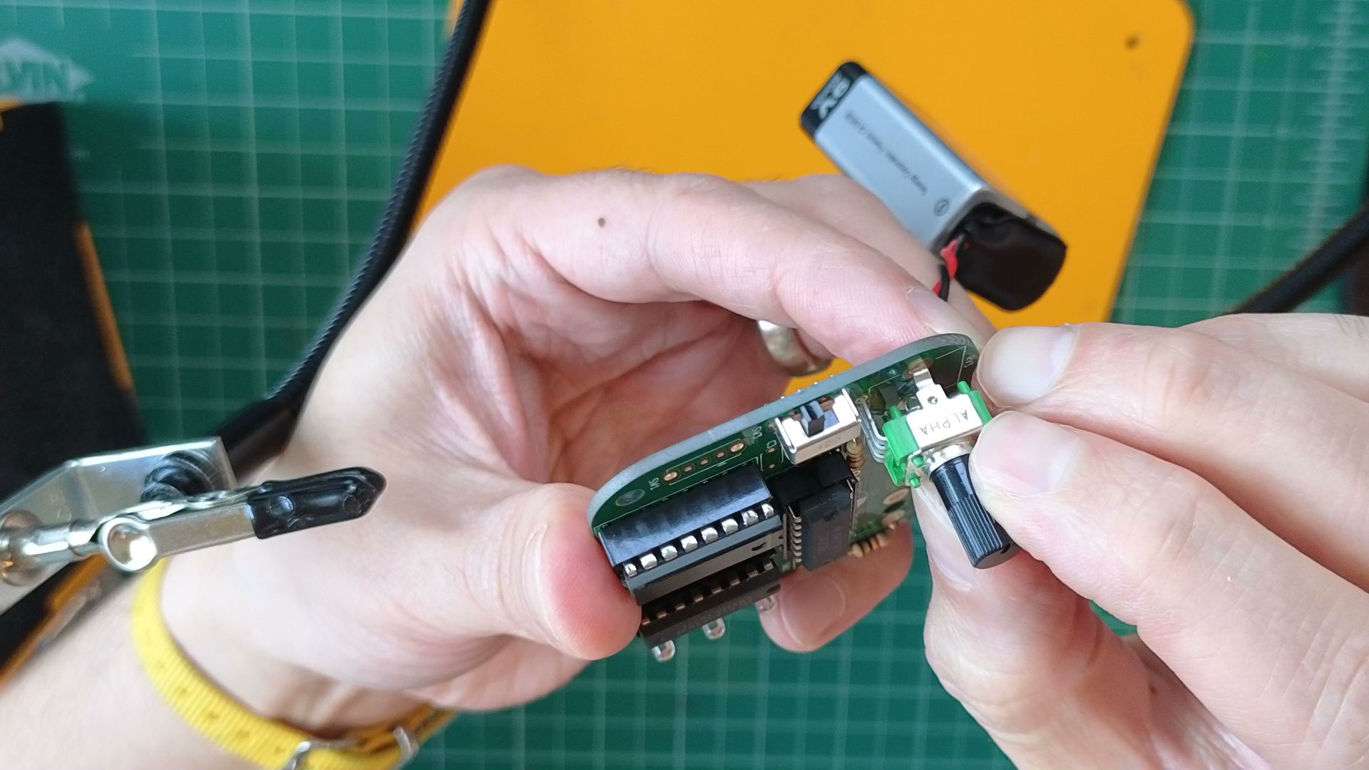
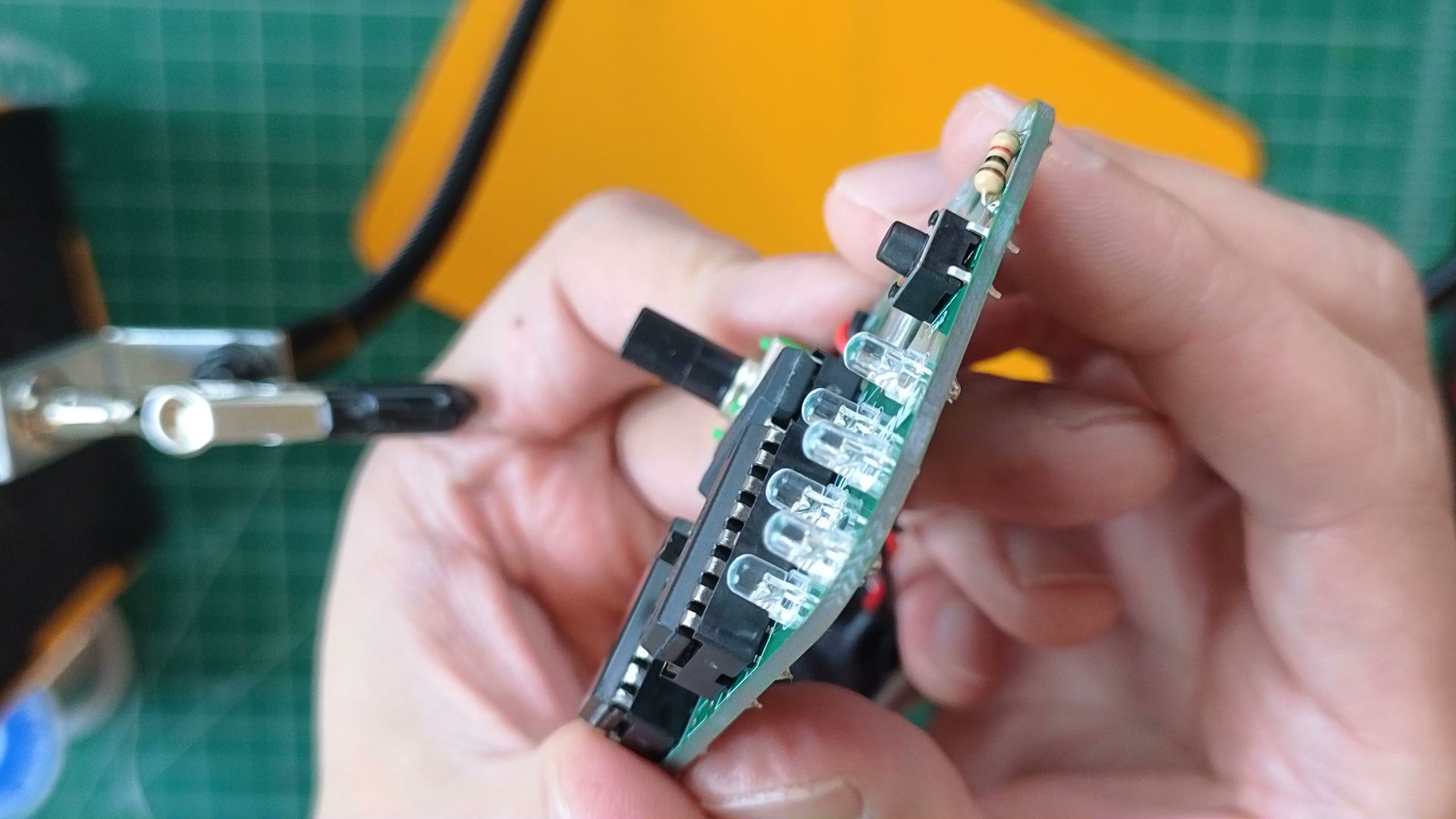
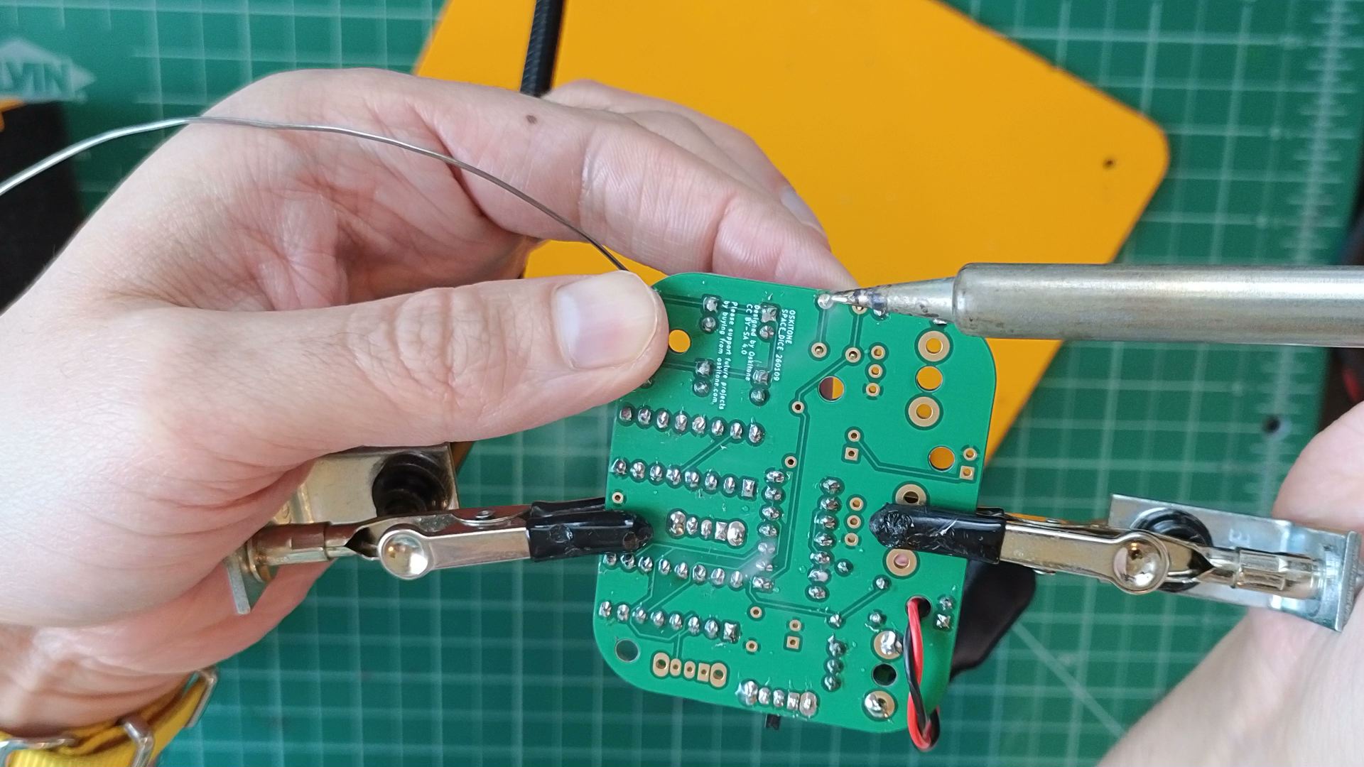
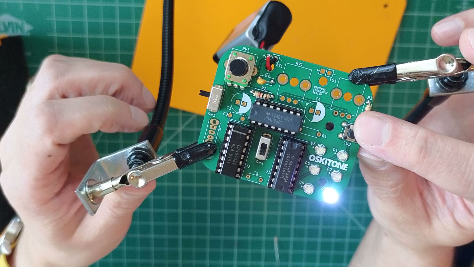
It's crucial that all sockets, potentiometers, and switches are perfectly flat against the PCB. Make sure they're fully in there before soldering all their pins.
Chips are labeled differently depending on their manufacturer and series. For example, the 4093 may say CD4093, HEF4093, or HCF4093BE, etc... What's important is the "4093" in the middle there.
Steps
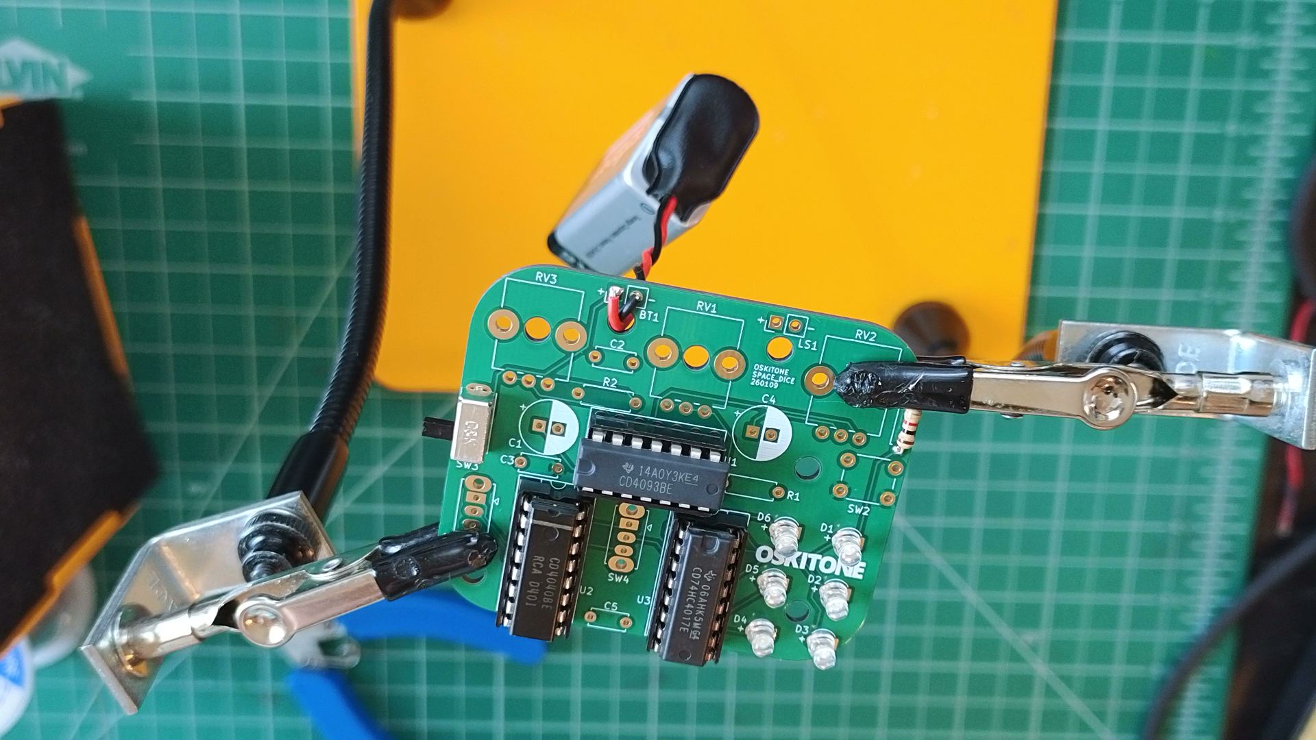
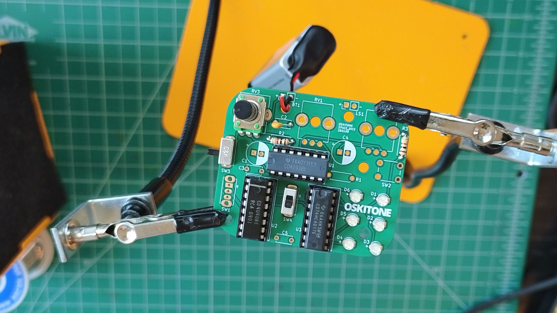
- Connect 4093
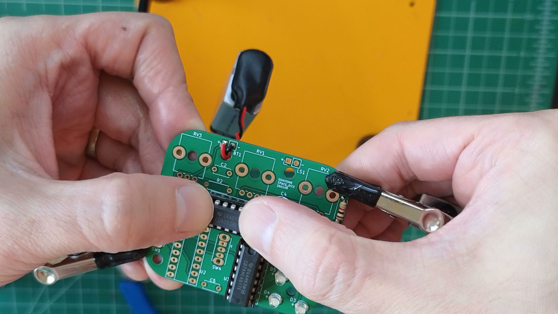
- Solder 14-pin socket to U1.
- Insert 4093 into socket.
- Connect 4040
- Solder 16-pin socket to U2.
- Insert 4040 into socket.

- Solder capacitor C2 (.1uF, marked 104) and resistor R2 1k (Brown Black Red).
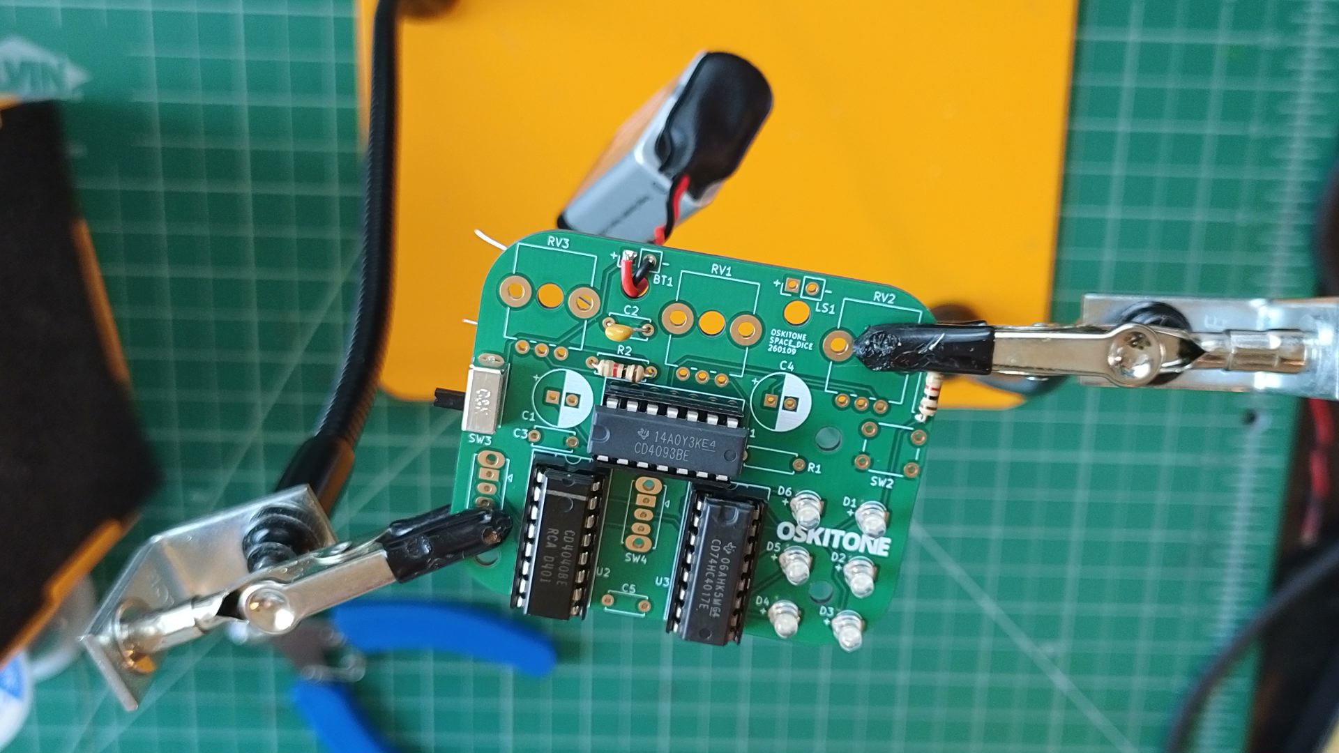
- Solder potentiometer RV3 10k (marked A10k)
- A trick to get the pot to snap in better is to gently pinch its tabs inward before popping it onto the PCB.
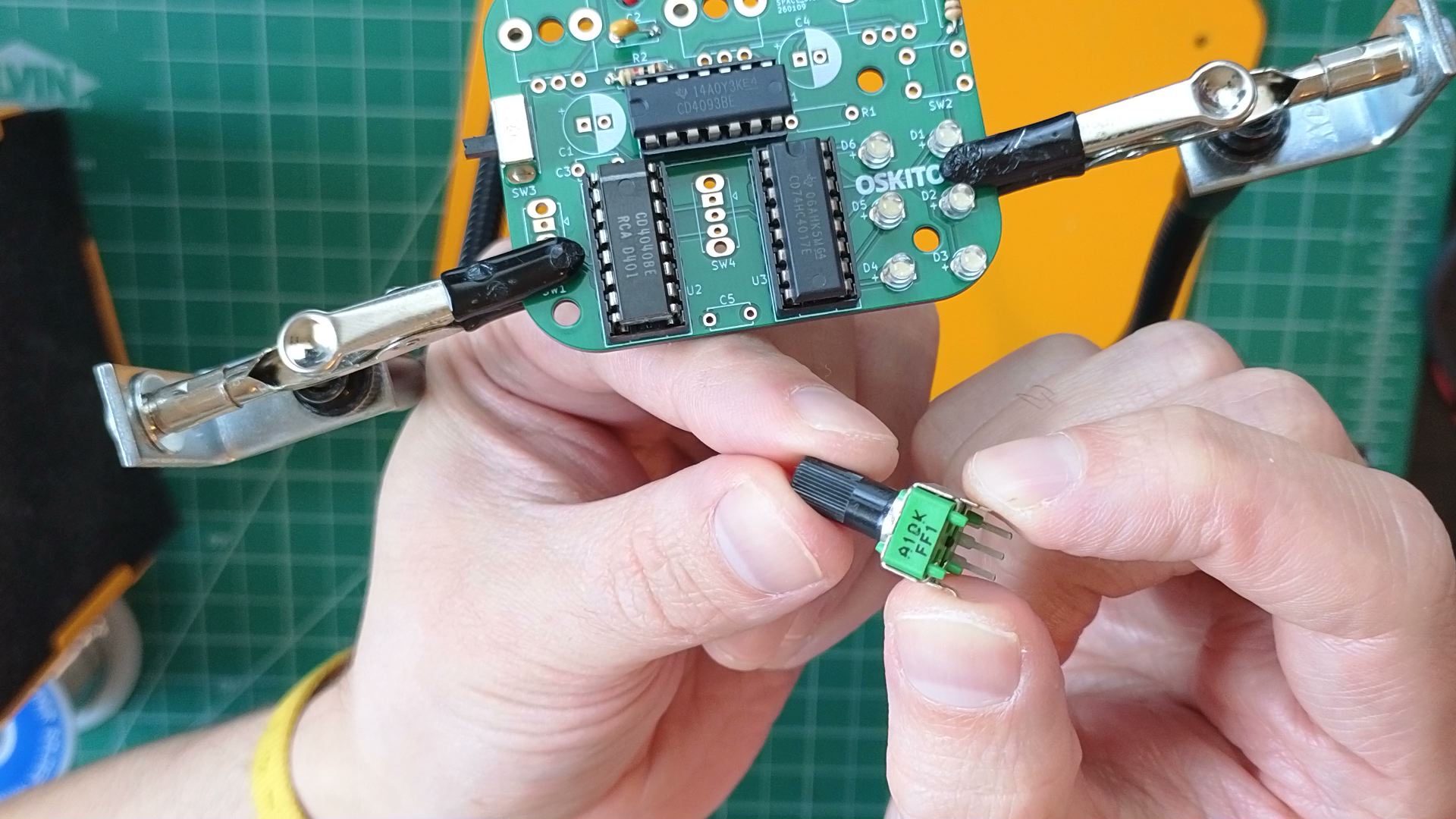
- A trick to get the pot to snap in better is to gently pinch its tabs inward before popping it onto the PCB.
- Solder vertical SPDT to SW4.

- Solder pushbutton SPST tactile switch to SW2.


Test
Press SW2. The LEDs should light up one at a time in a cycle, D1 through D6 and then looping back to D1. RV3 and SW4 should control how fast it loops.
The LED cycle will likely continue beyond (or even regardless of) SW2's pressing. Totally fine.
If an LED is getting skipped, it's probably in backwards.
Not working as expected? Check the PCB troubleshooting section. Otherwise, continue.
How it works
This summary introduces some BIG CONCEPTS, and, in an attempt to not be overwhelming, they're only briefly explained. It's okay to not understand them! When you're ready and curious, follow their links to learn more.

- The 4093 at U1 is a quad (ie, four) NAND logic gate chip, and U1A is one of gates. Logic gates are simple machines that take input(s), perform some function, and finally provide a new output.
- If you connect a 4093 NAND gate's output to one of its inputs with an RC network, you get a relaxation oscillator, controllable with the remaining input. Its frequency is set by C2, R2, and RV3. Later, the 3D-printed enclosure will label RV3 as "TONE."
- The oscillator clocks the 4040, another timer chip. Unlike the 4017 that counts in decimal with ten one-at-a-time outputs, the 4040 presents its count in binary with 12 many-at-a-time outputs.
- Each 4040 output pin is a binary digit (a bit!) and all of them together make a 12-digit number. The language of electricity is voltage, but for binary we use 1s and 0s. So it starts at
000000000000(ie, all GND) and increments at each clock pulse:000000000001(all GND except Q11 at VCC),000000000010(Q10 VCC),000000000011(Q10 and Q11 VCC),000000000100(Q9 VCC),000000000101, and so on. - The 4040s CLK input and Q outputs are square waves. If you were to measure the outputs' frequencies, you'd find that each is half the frequency of the pin before it. In other words, Q0 is half the input, Q1 is half Q0, etc. Give it a high frequency, it returns 12 lower frequencies. It's a prescaler!
- SW4 switches between two 4040 outputs to clock the 4017, which cycles its output LED lights. When SW4's actuator is up, the 4017 increments faster; when it's down, the 4017 increments slower. The enclosure labels this switch "INCR," short for increment speed.
- Like U3, U2's schematic layout is a rectangle that doesn't match its physical layout. The 4093 at U1, however, is even weirder... It's totally separate symbols! The 4093 is called a "Quad" NAND with four logic gates, but we're only using one for now. Its other three are unconnected, and its power pins are pulled out into its own block. This is pretty common for
Consider:
- Pressing SW2 triggers the oscillator to run, but why does it continue running afterwards? (Hint: the floating 4017 input from before)
- Our 4017 is reset by one of its output pins, but how is the 4040 reset?
- A 4017 that's not prematurely reset can count in decimal from 1 to 10. How would you represent that range in binary?
- The 4040 can count in binary from
000000000000to111111111111. How would you represent that range in decimal?